Inertial Sensors
Accelerometers, Gyroscopes, and More
The superb performance of MEMS sensors based on capacitive measurement technologies makes them highly suitable for detecting small changes in movement like thrust, velocity, angle and direction.
Types of inertial sensors
MEMS accelerometers can measure movement across one, two, and three axes, and multiple capacitor designs can decrease temperature dependence and cross-axis sensitivity while improving linearity.
MEMS gyroscopes are recognized as critical elements for navigation, orientation, and position sensing. They can detect signals as small as the earth's rotation and as large as tracking the motion of a human hand. MEMS gyroscopes have clear advantages with respect to small size/weight, low power, robustness in harsh environments and potential for volume manufacturability.
Our inertial sensor solutions include both gettered and getterless designs
-
MIDISTM Process Platform (getterless)
-
Super-MIDISTM Process Platform (getterless)
-
MicraSilQTM Process Platform (gettered)
Teledyne MEMS has deep experience in inertial sensors, including multi-axis and multi-function devices. Our portfolio includes milestones in miniaturization as well as some of the world's best vacuum and hermeticity capabilities. Our platforms have been developed specifically to allow users to design their own motion sensors using a stable, well characterized process architecture.
Teledyne has decades of high-volume manufacturing expertise of inertial sensors products. Our processes are developed with the highest quality standards in the industry. The reliability of our bond interfaces has been proven on multiple products.
Our Support for Your Designs
Our engineering team has decades of experience of solving the key challenges and optimizing yields of inertial sensors:
- Eliminating stiction in low-G accelerometers
- Reducing noise of low-frequency accelerometers
- Reducing quadrature errors and frequency splits in gyroscopes
- Maximizing Q-Factor of gyroscopes
We offer process design kits (PDK) to our customers to assist in their MEMS designs, which:
- Reduce initial development cost
- Improve electrical performance, reliability, and extensibility into 3D IC designs.
- Ensure high quality factor (Q-Factor)
- Accelerate manufacturing ramp
- Simplify board reflow mounting to ensure performance of entire application
- Open up custom device layer options
What is an Inertial Measurement Unit (IMU)?
Three-dimensional IMUs provide specific force, angular rate, and orientation information using a combination of accelerometers and gyroscopes. They can also incorporate additional sensors like to provide even more functionality. Their tiny size and high precision have won them a place in a huge variety of applications.
IMUs are used to improve the interactivity of phones, tablets, and AR/VR headsets as well as precisely measuring activity in sports- and health-related devices like smartwatches and medical trackers. IMUs are also used to maneuver a wide range of modern vehicles, from cars and motorcycles to aircraft, UAVs, and satellites.
MIDIS Process Platform
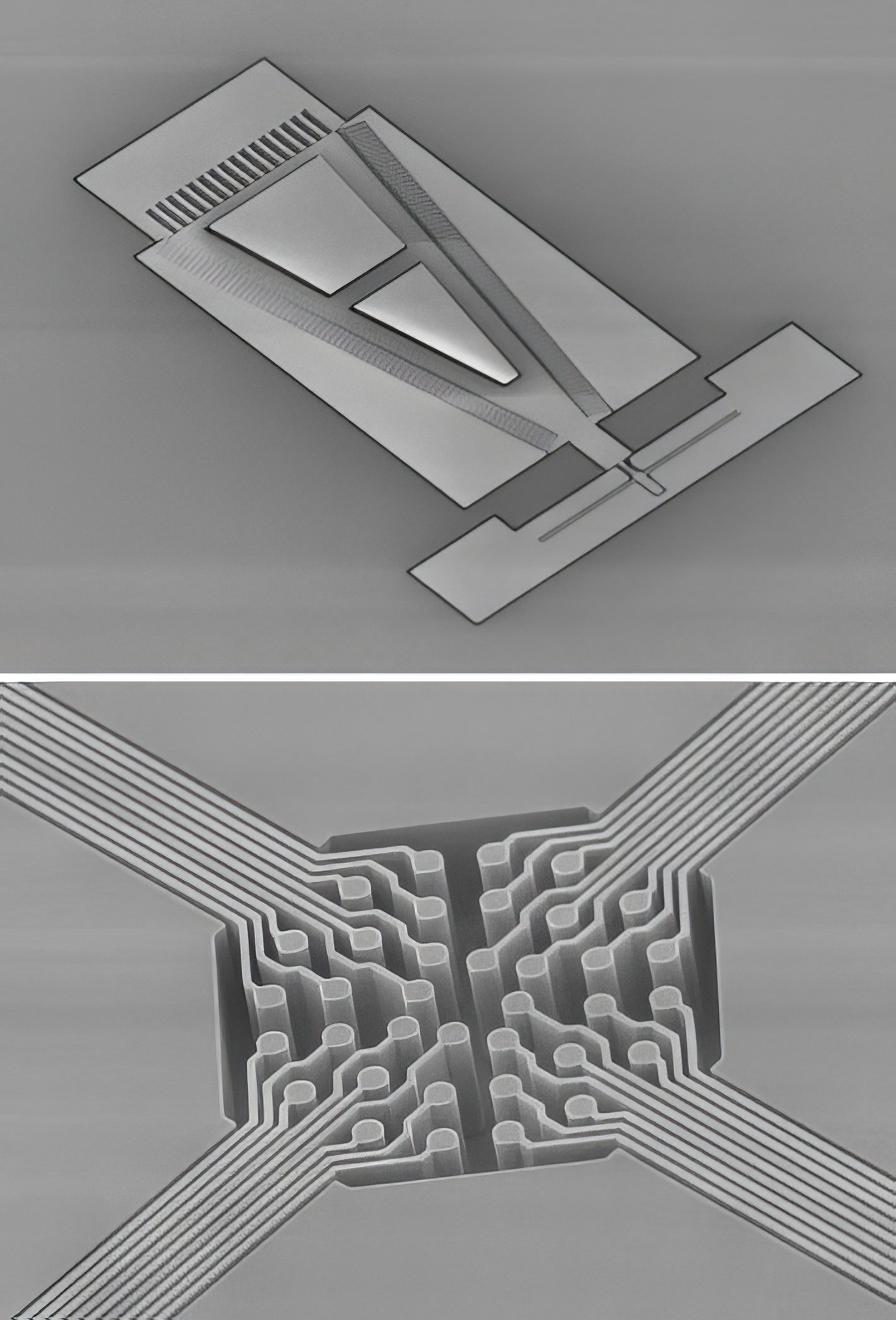
MIDIS (MEMS Integrated Design for Inertial Sensors) is a proven microfabrication platform for the high-volume and low-cost manufacturing of accelerometers and gyroscopes for integrated motion units (IMUs), a crucial component of today’s consumer electronics. The MIDIS platform breaks the one-process-per-product MEMS paradigm, greatly reducing development cost and time-to-market.
Implemented in a volume-compatible 200mm wafer diameter production environment, the process enables considerable flexibility to support a broad range of device designs, facilitating the rapid transition of new device concepts to volume production.
Key Process Features
- Getter-less, integrated wafer-level high-vacuum hermetic package with c-Si TSV
- Base pressure < 0.5 Pa (for gyroscope), customizable pressure level for damped accelerometers.
- All silicon features in the cavity, high temperature fusion bond to seal cavity (high Q-Factor, high hermeticity, high frequency stability over time).
- 11 mask process, 1.5 μm feature size in a 30 μm crystalline silicon layer (AR 20:1)
- High uniformity residual pressure and resulting Q-Factor (Some designs demonstrate > 250,000)
- Smaller die size through aggressive lithography features and TSV
- Single Die / 6-Axis combo sensors (3-Axis Gyroscopes & 3-Axis Accelerometers)
- Wafer-Level CMOS ASIC Integration (200mm Wafers)
- Design Kit (CAD Tools, PDKs)
Target Markets
- Consumer
- Industrial
Super-MIDIS Process Platform
The process builds on all the advantages of the MIDI platform and takes them even further. Performance and precision upgrades allow for the incorporation of advanced design elements specifically designed to meet mission-critical challenges.
Navigation-grade inertial sensors offer a much higher performance envelope, finding integrations autonomous advanced systems like UAVs and other vehicles.
Key Features
- 18 μm feature size in a 270 μm crystalline silicon layer (AR15:1), with larger proof mass enabling higher sensitivity and lower noise
- Double electrode and routing layer integrated inside the cavity
- Cap heater and thermal sensor options to regulate temperature
- All features of MIDI Process Platform
Target Markets
- High-Performance Industrial
- Tactical and Law Enforcement
- Aerospace Navigation
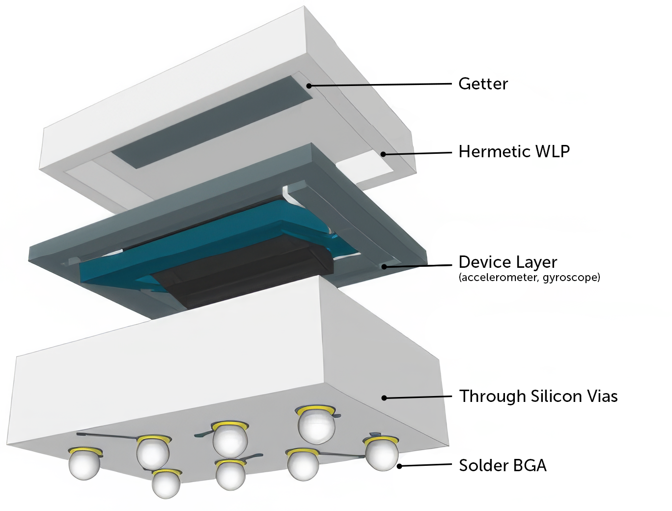
MicraSilQ Process Platform
Our MicraSilQ wafer-level packaging (WLP) process platform provides an all-in-one solution for integrating wafer level fabrication, hermetic packaging, and through-silicon-via (TSV) architecture.
Like our other options, this process offers you an established and reliable process for a fast ramp to manufacturing. MEMS inertial sensors can be sensitive to PCB design and mounting processes, but simplified board reflow mounting minimizing stresses to the MEMS package, ensuring the best performance for the entire application. A custom device layer opens up new possibilities for unique applications.
MicraSilQ Features
- Insulated Through Silicon Vias (TSV) – polysilicon filled
- Thick silicon device layer (60 μm standard) for high comb finger capacitance
- Lead-free solder ball grid array
- Hermetic seal with enclosed getter
Process Design Kit
The MicraSilQ PDK reduces initial development cost, ultimate manufacturing component cost, footprint, thickness and weight, while simultaneously providing improved electrical performance, reliability, and extensibility into 3D IC designs. The result is drastic cost reduction and MEMS package size miniaturization.
Teledyne MEMS Capabilities
We offer the combined expertise of more than 120 engineers and scientists in development and process modules, backed by an organization with more than 25 years of microfabrication innovation and problem solving. With deep expertise across automotive, commercial, medical, telecom, industrial sensor products, we can here to help you realize your ambitious new products and business plans.
We blend MEMS applications experts together with process performance champions to design process flows for robust, cost-effective fabrication to match customer requirements. Our project teams strive for deep insights to their customers’ needs and close communications throughout the relationship. Learn more about our capabilities.

Do you have any questions?
Select Teledyne as your partner to move your MEMS device from concept to mass production.
Contact usStay connected
The MEMS industry is evolving quickly with new innovations, applications, and events. Subscribe to our newsletter and we’ll help you keep up to date with the latest developments
Subscribe